 |
Semiconductorsuctors 
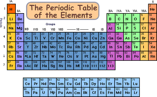
Much of chemistry is devoted to the study of carbon based compounds because carbon can form vast complex molecules. It is capable of doing this because of its four valence electrons. Silicon and germanium are also in group IV and they too can form complex structures. All group IV elements can be made to conduct electricity, even carbon, which is a non-metal.
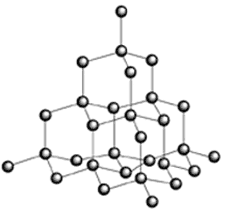
Silicon is essentially non-metallic whereas germanium is metalloid and tin and lead are metals.Germanium and silicon ore called semi-conductors. A semi-conductor has a higher conductivity than an insulator and a lower conductivity than a conductor. They have a negative temperature co-efficient of resistance (i.e. as temperature increases, resistance decreases. Compare this with metals which are the opposite. At low temperatures some metals (tin and lead being two of them) exhibit superconductivity: their resistance becomes virtually zero as the temperature of absolute zero approaches). Pure elements that form semiconductor crystals are termed INTRINSIC semiconductors as their semiconductor nature is inherent. Silicon is second only to oxygen in weight percentage of the earth's crust (= 28%) whereas germanium is relatively rare. Within the pure germanium or silicon crystal inter-atom bonds form a vast structure similar to that of diamond (covalent tetrahedral 3-D formation of strong bonds). NB They cannot form a graphite-like structure; that is unique to carbon. Carbon has two resistivities
(one for graphite, one for diamond). Taking diamond as the 'normal' structure,
electrical resistivity decreases down the group from and insulator (diamond)
through semiconductors (silicon and germanium) to metals (tin and lead).
(Graphite's resistivity comes between germanium and tin as it is a poor
conductor rather than a semiconductor). In pure germanium (or silicon) crystals the valency electrons bond with neighbouring atoms to form a stable 3-D covalent lattice. High energy electrons within these bonds can free themselves from the structure to form conduction electrons, leaving positive 'holes' which could be viewed as positive charge carriers. If heat energy is given to the structure more electrons become free and more holes are formed so the resistivity decreases (or conductivity increases) hence the negative temperature co-efficient of resistance. Insulators also have a negative temperature co-efficient of resistance. Above 100'C the lattice breaks down completely and so temperature is an Important factor when using semiconductor materials. The conductivity of semiconductor materials can be increased without raising temperature by DOPING. Doping consists of introducing impuity atoms into the structure. These Impurities are usually from groups III or V. Those from group V have a surplus valence electron when they are bonded within the group IV element's crystal structure. (NB they haven't an overall charge, Just an un-bonded electron). So if phosphorus (P), Arsenic (As) or Antimony (SB) atoms are introduced into the lattice they are able to donate electrons to be conduction electrons and increase the conductivity of the crystal (they do not make it negative!!) they are therefore called DONOR atoms. The semiconductor has gained negative charge carriers and is therefore called an n-type semiconductor. Those from group III have a missing valence electron when they are bonded within the group IV element's crystal structure. (NB they haven't an overall charge, they are Just an electron short to fit in with a quadravalent structure). So if boron (B), Aluminium (Al), Gallium (Ga) or Indium (In) atoms are introduced into the lattice they produce holes in the lattice. These holes mop up stay conduction electrons that left their original position because of surplus energy. Thus holes 'move' like positive charge carriers because holes move in the opposite direction of electrons. A small amount of dopant causes a very large number of holes compared to the number of free electrons in the pure or 'intrinsic1 semiconductor. Thus the charge carriers are increased, but they are positive charge carriers and the conductivity of the crystal increases (they do not make it positive!!). They accept electrons into the holes and they are therefore called ACCEPTOR atoms. The semiconductor has gained positive charge carriers and is therefore called a p-type semiconductor. The
charges balance in a semiconductor - it does NOT have a net charge! |
Follow me...
|


Cyberphysics - a web-based teaching aid - for students of physics, their teachers and parents....